Advantages:
- Creates ultra-smooth nanoribbons quickly, no costly chemicals or cleanrooms needed.
- Cuts manufacturing costs while boosting device performance and reliability at scale.
- Works with multiple materials, from graphene to quantum-grade semiconductors.
- Eco-friendly process that is easy to adopt for advanced electronics production.
Summary:
Traditional nanoribbon fabrication relies on complex chemical treatments and vacuum-based techniques that are expensive, slow, and difficult to scale. These methods often produce inconsistent results, limiting commercial adoption and slowing innovation in the semiconductor and quantum industries that demand precision, uniformity, and efficiency at the nanoscale
Our researchers have created a breakthrough mechanical fracture process that produces highly aligned, atomically smooth nanoribbons in a clean, scalable, and cost-effective way. The method eliminates hazardous steps while ensuring uniform quality, making it ideal for companies seeking reliable, high-performance materials for nanoelectronics, quantum sensors, and advanced computing devices.
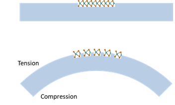
Schematic illustration of using mechanical fracture to generate nanoribbons from nanoflakes.
Desired Partnerships:
- License
- Sponsored Research
- Co-Development