Advantages:
- Enables scalable, atomic-level additive and subtractive manufacturing
- Uses naturally occurring misalignments (incommensurabilities) to guide ultra-precise patterning
- Supports inverse design using machine learning for targeted feature control
- Opens pathways to advanced applications in quantum devices and molecular separation
Summary:
Advanced manufacturing at the atomic scale faces steep challenges existing top-down and bottom-up techniques cannot reliably produce Ångstrom-level precision over large areas. The resolution limits of lithography and the uncontrollable nature of self-assembly restrict the creation of nano-features needed for next-generation devices and materials. As miniaturization approaches fundamental limits, there's a pressing need for new strategies that turn material imperfections into tools for precision.
This technology introduces a novel approach to manufacturing using incommensurate stacking of two-dimensional layered materials (2DLMs) to form moire patterns engineered surface states that guide Ångstrom-precise additive and subtractive processes. By selectively modifying these patterned domains with chemical reactions or plasma etching, the method produces uniform nano-pores, nano-channels, and nano-islands across large areas. A machine learning framework supports inverse design, using experimental data to predict processing pathways for desired structures. The technology enables manufacturing of high-performance separation membranes, spin-based quantum devices, and next-gen biosensors addressing strategic needs in semiconductors, clean energy, and national security.
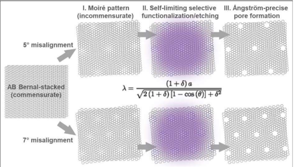
This image shows how Angstrom-precise pore arrays are formed in 2D layered materials by combining rotational misalignment, selective functionalization, and plasma etching. The resulting moire-guided process enables precise, scalable nano-patterning at the atomic level.
Desired Partnerships
- License
- Sponsored Research
- Co-Development